Compensation Design for Peak Current-Mode Buck Converters
Abstract
Peak Current-Mode Controlled Buck Converters are currently
very popular and widely adopted in consumer electronics and computer peripheral
power management. This application note presents a design procedure for feedback
compensation of peak current-mode buck converters, and also introduces the SIMPLIS
tool for circuit simulations and the Mathcad mathematical software for quantitative
design, and finally provides the verified results by actual measurements.
1. Open-Loop Analysis of Peak Current Mode Buck Converters
Peak current-mode control is implemented by an inner current loop, composed
of a current sensing circuit, Ri, with a slope compensation (saw-tooth ramp)
circuit. The sensed current ramp is summed with the saw-tooth ramp, and then
is compared with the output of the error amplifier, VC. And the result is used
to control the ON-time, TON, of the MOSFET. The circuit diagram is shown in
Figure 1.
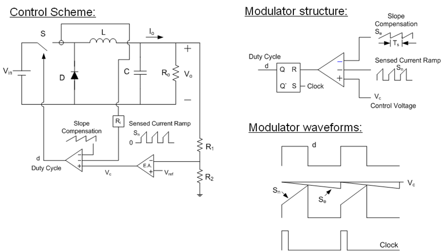
Figure 1. The circuit diagram of a peak current-mode buck
converter
For peak current-mode, sub-harmonic oscillation may occur for duty cycle
D > 0.5. In Figure 2, TON is the ON-time of the MOSFET, and TS
is the switching period; the dashed line is for the perturbed inductor current,
and the solid line is for the ideal steady-state inductor current. For D <
0.5, if a perturbation is initiated, it will be completely damped after a few
cycles; that is, an unstable state caused by the perturbation will gradually
be stabilized. However, for D > 0.5, if a perturbation is initiated, it will
continue to increase for the next few cycles, which makes the system unstable.
Slope compensation is therefore introduced to eliminate the risk of this sub-harmonic
oscillation so that the system can remain stable. Slope compensation is implemented
by adding a saw-tooth ramp of the same frequency as of the control circuit to
the sensed inductor current ramp so that the system can still be stable at duty
cycle above 0.5.
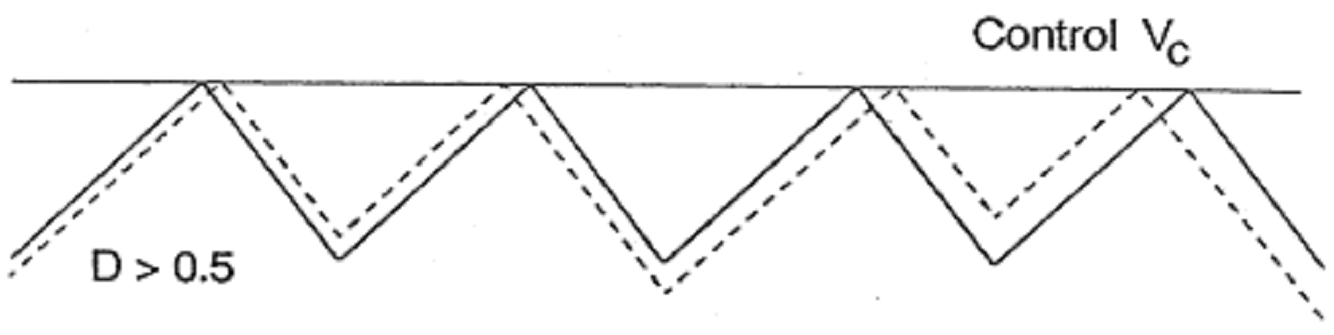
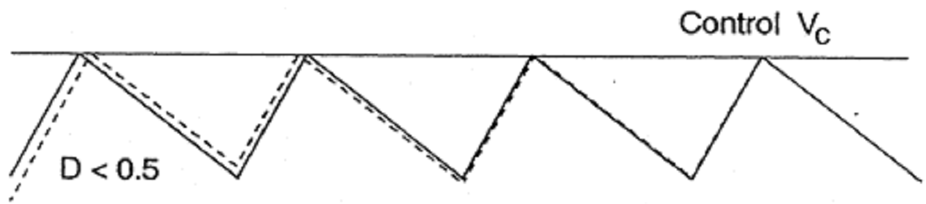
Figure 2. The sensed inductor current ramps by Ri at duty
cycles D < 0.5 and D > 0.5
The small-signal model of a peak current-mode buck converter [1] [2] will
be introduced in this section. The Buck PWM Switch Model, proposed by V. Vorperian
[1] and the small-signal model for peak current-mode control, by Raymond B.
Ridley [2] are displayed in Figure 3. The equations derived according to the
model will be applied in compensation design for peak current-mode buck converters.
Figure 3. The Buck PWM switch model and the small-signal
model for peak current-mode control
The open-loop transfer function of a peak current-mode buck converter is
listed below [1], [2]:
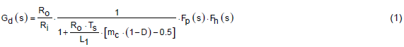
Fp(s) in Equation (1), which dominates the open-loop low-frequency
characteristics of this configuration, is shown below, as Equation (2), which
has a zero and a pole.

Fh(s) in Equation (1) represents the high-frequency characteristics
of this configuration, where the current-sense transformer Ri plays an important
role. Fh(s) is described below, as Equation (3) and it has two high-frequency
poles.
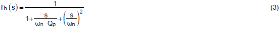
Figure 4 shows a low-frequency dominant pole (at a slope of -20dB / decade),
and a high-frequency double pole (at a slope of -40dB / decade decaying). The
ESR zero in between is from the ESR of the output capacitor.
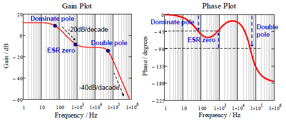
Figure 4. The Bode plot of the open-loop peak current-mode
buck converter
The equations for compensation design will be analyzed step by step as follows:
To begin with, the equation of the exact low-frequency pole is presented
below:

Advanced computational tools will be needed to calculate for the above equation.
However, the simplified equation, listed below, is a close approximation, by
which the pole can be found quickly.

The equation below is for the output capacitor zero:

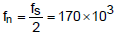
The following equation is for the double pole, positioned at the half of
the switching frequency:

With the equations above, a design example will be offered to describe the
important characteristics of a peak current-mode buck converter.
Figure 5
displayed the circuit diagram and the corresponding circuit parameters of a
buck converter. The input voltage is 12Vdc, the rated output current 3A, the
output voltage 3.3V, the operating frequency 340kHz, the inductance 10μH,
the output capacitance 44μF, and its ESR 5mΩ.

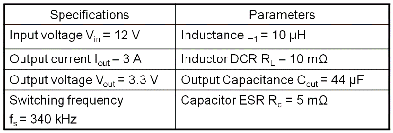
Figure 5. The circuit diagram and the corresponding circuit
parameters of a peak current-mode buck converter.
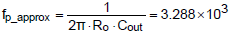
Substitute the above parameters to Equation (4) to obtain a more accurate
low-frequency first-order pole, which is located at 4.3kHz.

Slope compensation factor, mc, is defined as ,
where Se is the slope of the added compensation saw-tooth ramp and
Sn the slope of the sensed current ramp when the switch is on.
,
where Se is the slope of the added compensation saw-tooth ramp and
Sn the slope of the sensed current ramp when the switch is on.

By Equation (5), the first-order pole, 3.3kHz, can be readily calculated
as below.
Substitute the above parameters to Equation (6), and the exact location of
the output capacitor ESR zero can be found as 723kHz.
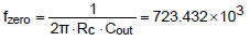
Then, by Equation (7), the high-frequency double pole is obtained as 170kHz.
With all the parameters above plugged in, a Bode plot can be drawn by Mathcad
as below. In Figure 6, it can be seen that a pole occurs at low frequency (3.28kHz), and ESR zero (723kHz) occurs at an even higher frequency than the double
pole, since the smaller ESR is used.
Figure 6. The Bode plot of the open-loop peak current-mode
buck converter in the design example
2. Compensation Design of Peak Current-Mode Buck Converters
The previous section has described the characteristics of a peak current-mode
buck. In this section, how to compensate peak current-mode buck converters for
system stability will be investigated. In Figure 7, the open-loop gain is plotted
in red; at low frequencies, the DC gain is low. Low DC gain at low frequencies
can cause steady-state errors, which can be seen in Figure 10, for which the
frequency responses of two different DC gains with the same bandwidth and phase
margin are displayed in Figure 9. For f > fc, the gain curve is
at the slope of -40dB / decade, and the phase curve is at the slope of -90°/
decade, which often results in insufficient phase margin, illustrated in Figure
8, which furthermore causes system instability. The optimal closed-loop gain
is drawn in blue. Compared with the open-loop gain, the closed-loop gain manifests
the following advantages: higher DC gain at low frequency so that the steady-state
errors can be minimized as in Figure 10, and for f > fc, the gain
is at the slope of -20dB / decade, and the phase -45°/ decade, as shown
in Figure 7, thereby to improve the phase margin (P.M.).
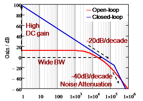
Figure 7. The comparison of the open-loop and closed-loop
Bode plots
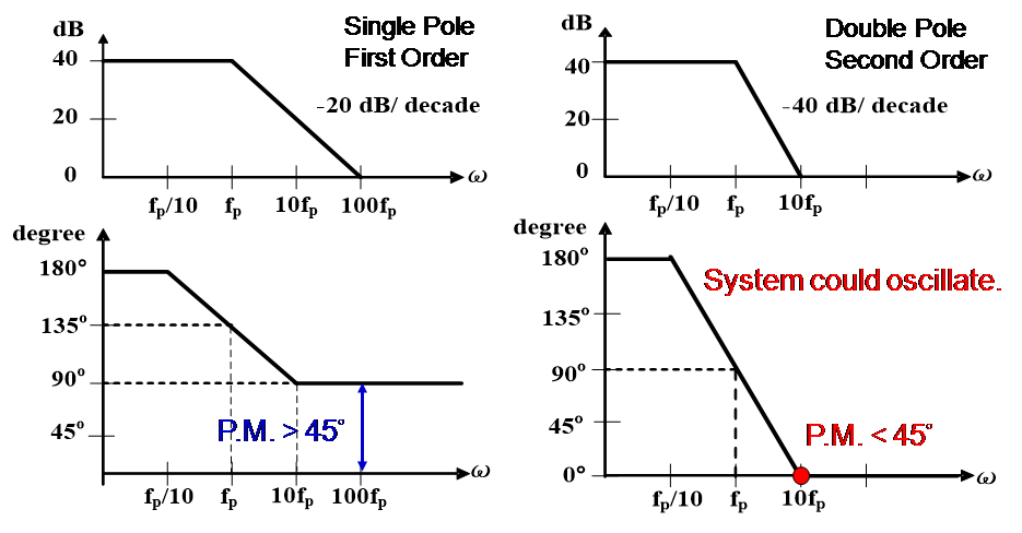
Figure 8. Single pole vs. double pole
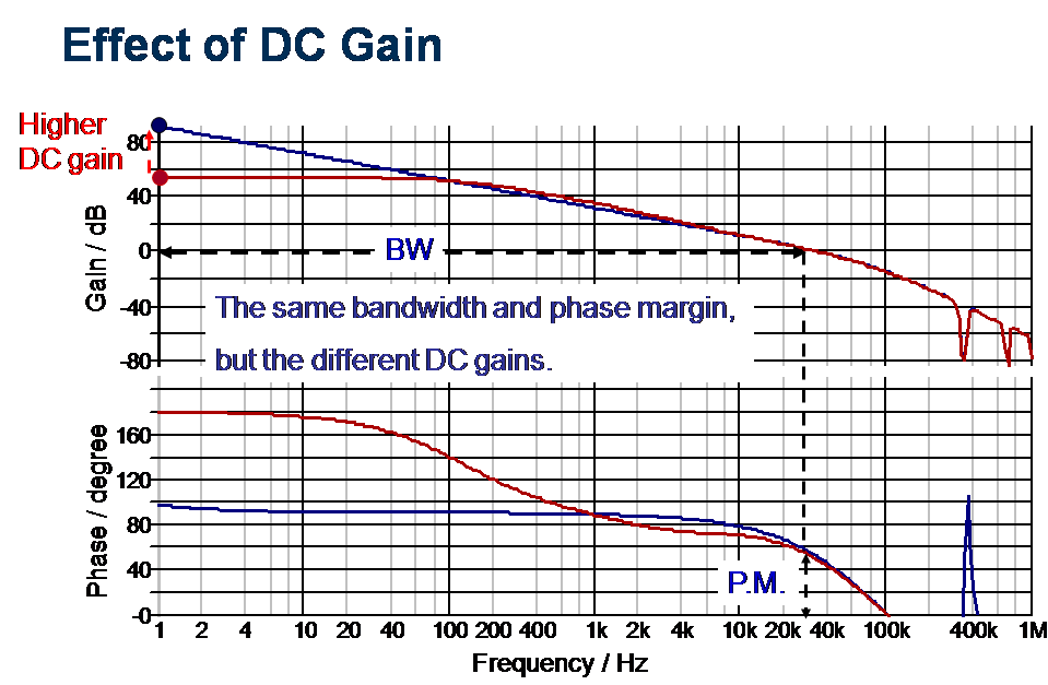
Figure 9. Different DC gains with the same bandwidth and
phase margin
In Figure 10, it can be seen load regulation is better
with higher DC gain, and worse with lower DC gain.
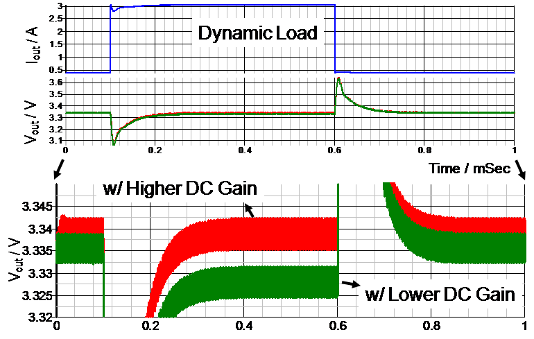
Figure 10. The effect of DC gains on load regulation
Based on the above analysis of the circuit parameters on system performance,
what is needed for a compensator is a zero to cancel the low-frequency pole
of a peak current-mode buck converter, as in Figure 11, so that the gain curve
will be at the slope of -20dB / decade at the crossover frequency, thereby to
achieve a better phase margin. At high frequencies, a high-frequency compensator
pole can help filter out high-frequency noises.
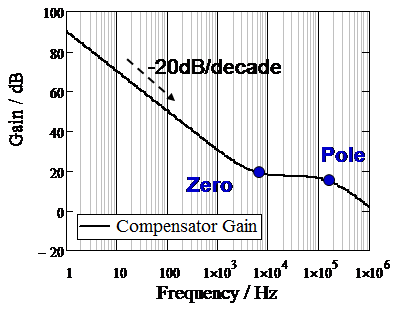
Figure 11. A compensator offers a zero and a pole
Take a GM-Type compensator below as an example. Since a GM-Type compensator
has one zero and two poles, it is quite suitable to compensate peak current-mode
buck converters. First pole can be obtained from Rgm and Ccomp,
the other pole from Rcomp and Cgm, and a zero from Rcomp
and Ccomp.
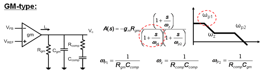
Figure 12. A GM-Type compensator
Compensator Design Procedure :
Step 1 :
Set the crossover frequency (i.e. the bandwidth). In the example
above, the operating frequency is 340kHz, and the bandwidth is usually set
as 1/10 of the operating frequency.

Step 2 :
Set the zero of the compensator to cancel the pole of the peak
current-mode buck topology.

Step 3 :
The compensator pole is set to the lower frequency among the ESR
zero and 1/2 of the operating frequency. In this example, 1/2 of the operating
frequency is lower than the ESR zero, so set the compensator pole to 1/2 of
the operating frequency.

Step 4 :
By Mathcad, the phase margin of 48° can be obtained by the
following equation. Usually for stability, the phase margin should be greater
than 45°.

Step 5 :
From Equation (12), the DC gain, increased by the compensator
at the crossover frequency, can be calculated as 17.4dB.

Step 6 :
The parameters of the compensator in this example, such
as Rcomp = 5.9kΩ, Ccomp = 6.23nF, Cgm
= 158pF, can all be obtained as follows.
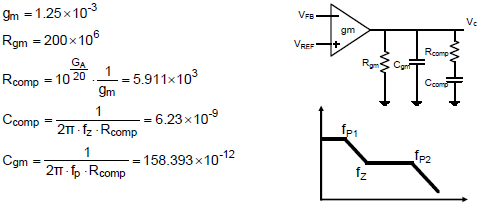
Step 7 :
Substitute all the above numbers into Equation (13), then enter
the equation into Mathcad, and the Bode plot of the compensator can be drawn,
seen in Figure 13.
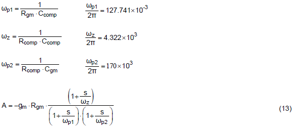
Figure 13. The Bode plot of the compensator
3. The Closed-Loop Analysis of Peak Current-Mode Buck Converters
In this section, the SIMPLIS tool is used to simulate the peak current-mode buck converter and to substantiate the closed-loop frequency response analysis. The SIMPLIS schematic is displayed in Figure 14. The closed loop of this current-mode buck converter incorporates a current sensor, a compensator, and a slope compensation circuit.
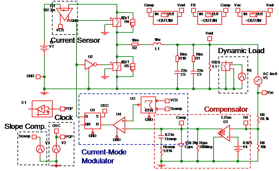
Figure 14. The SIMPLIS simulation shematic (the closed-loop peak current-mode buck converter)
In Figure 15, the equation from the previous section (red line) is drawn by Mathcad, which is verified with the simulation result (blue dots) of the SIMPLIS schematic in Figure 14. It demonstrates that the simulation result closely aligns with the analytical result, derived by Mathcad, and the bandwidth and phase margin are 34kHz and 48.9° respectively.
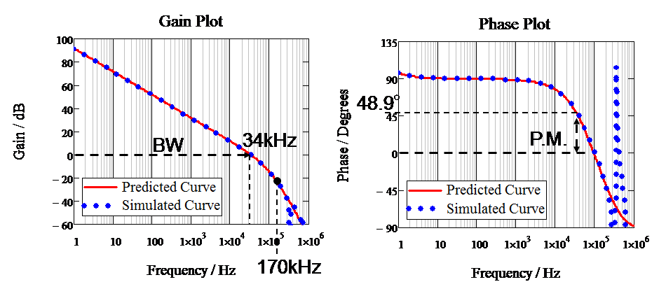
Figure 15. The comparison of theoretical analysis with the Matchcad and the SIMPLIS simulation
Figure 16 has exhibited the benefits a compensator can provide. First, a compensator (black dashed line) enhances DC gain in the low frequency range. The open loop response (red line), combined with the compensator response (black dashed line), makes the closed loop response (blue line). Second, a compensator increases bandwidth, as in Figure 16, the crossover frequency in blue is greater than that in red. Third, a compensator adds one high-frequency pole, which improves high-frequency noise immunity (at high frequency, the blue line drops faster than the red line). Fourth, the zero of a compensator helps achieve a sufficient phase margin.
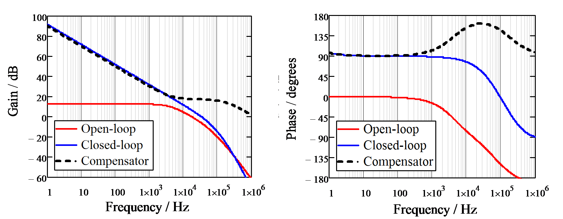
Figure 16. The comparison between the open loop and the closed loop
An actual measurement setup is presented in Figure 17, and an AC perturbation signal is injected into point R. The gain and phase plot can be obtained by measuring the output (point A) versus the input (point R). From the right-hand plot of Figure 17, the measured result (green line) shows good agreement with the analytical result (red line).
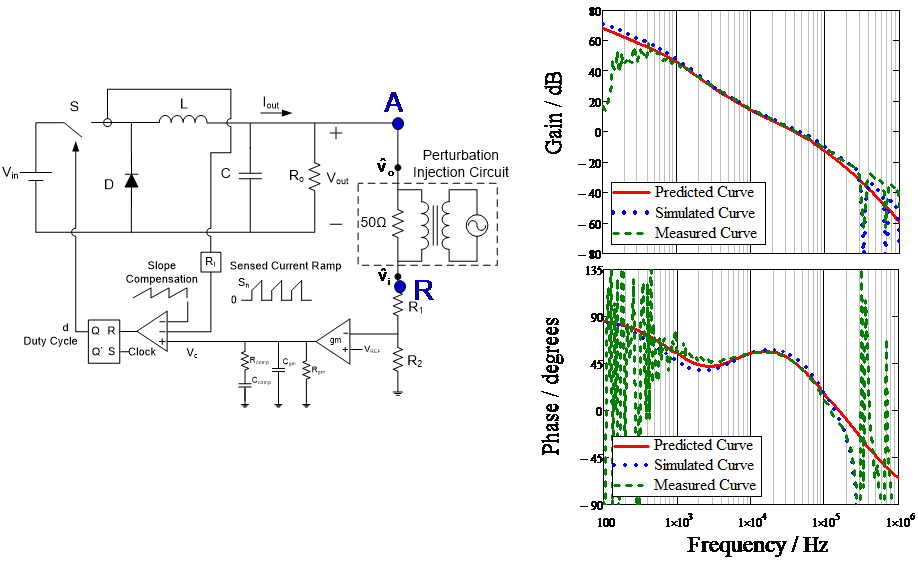
Figure 17. The experimental results verify the closed loop frequency response
4. Conclusion
- At low frequencies, an open-loop peak current-mode buck converter is still a single-pole system since the loop control is realized by injecting current signals into the loop only.
- Its compensator is easy to design. The compensator zero is designed to cancel the dominant pole of a buck converter for system stability.
- In order to assure sufficient phase margin, the design goal is that the gain curve is at the slope -20dB / decade, when passing the crossover frequency.
5. References
[1] V. Vorperian, “Simplified analysis of PWM converters
using model of PWM switch part I: continuous conduction mode,” IEEE Trans. on
Power Electronics, vol. 26, no. 3, pp. 490-496, May 1990.
[2] Raymond B. Ridley, A New Small-signal Model for Current-mode
Control, Ph.D. Dissertation, Virginia Polytechnic Institute and State University,
Nov. 1990.